Patterned Doping for Constructing 2D Lateral p-n junction via Ion Implantation

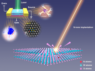
The schematic diagram of low-energy ion implantation constructing WS2 lateral p-n homojunction
USA, August 31, 2024 /EINPresswire.com/ -- For the practical application of 2D semiconductors, it is crucial to construct high-quality p-n junctions. Scientist in China developed a low-energy ion implantation system for constructing 2D lateral p-n homojunction. The conductivity type of WS2 was successfully realized to transform from n-type conduction to p-type conduction, and the universality of this method was demonstrated. The photodetector based on WS2 lateral p-n homojunction exhibits satisfactory self-powered photodetection ability. This achievement provides an effective way for controllable doping of 2D materials.
The feature size of silicon-based transistors is approaching the theoretical limit, which puts forward higher requirements for the “atomic level manufacturing” of semiconductors. The basic idea of “atomic level manufacturing” is to process and manipulate matters with atomic level precision, which will greatly reduce the power consumption of the chip and achieve a huge increase in the chip’s arithmetic power. 2D materials are expected to address the challenges faced in traditional silicon-based semiconductor devices. The p-n junction is the basic unit of optoelectronic devices in the information age. Previous studies have shown that 2D vertical p-n junctions can be prepared simply regardless of lattice mismatch. However, due to the van der Waals gap in interfaces and the impurities introduced in the stacking process, 2D vertical p-n junctions will reduce the carrier mobility. 2D lateral p-n junction can effectively solve these problems. Therefore, how to realize the construction of high-quality 2D lateral p-n junction is crucial for the practical application of 2D semiconductors. Ion implantation technique is a mature doping method for constructing p-n junction in traditional semiconductor industry, which has the merits of controllable doping concentration and depth, abundant doping elements, uniform doping area and non-polluting doping process. However, due to the high energy of incident ions (tens of keV), the traditional ion implantation technique will cause damage or even penetrate the atomically thin 2D materials during the implantation process, resulting in device failure. Therefore, it is difficult to directly modulate the electrical and optical properties of 2D materials using conventional ion implantation.
In a new paper (https://doi.org/10.1038/s41377-024-01477-3) published in Light Science & Applications, a team of scientists, led by Professor Xiangheng Xiao from School of Physics and Technology, Key Lab of Artificial Micro- and Nano-Structures of Ministry of Education, Wuhan University, Wuhan, China, has developed a low-energy ion implantation system for constructing 2D lateral p-n homojunction. Low-energy ion implantation technique inherits the advantages of the traditional ion implantation technique. It has a lower ion energy and shallower implantation depth, which is expected to address the problem that traditional ion implantation technique cannot be directly applied to modulate the performance of 2D materials. Although a few groups have conducted research on low-energy ion implantation, they have mainly focused on the microscopic characterization and defect modulation. To date, there is a lack of research on using low-energy ion implantation to achieve patterned p-type doping on 2D materials to completely reverse their conductivity types and construct lateral p-n homojunctions. By precisely modulating the implantation dose, the conductivity type of the WS2 flake is successfully modulated, which could be converted from n-type to bipolar or even p-type. The universality of this method is also demonstrated by extending it to other 2D semiconductors. In addition, the photodetector based on WS2 lateral p-n homojunction exhibits satisfactory self-powered photodetection capability. This work provides an effective method for controllable doping of 2D materials and promotes the practical application of 2D materials.
The authors used the low-energy ion implantation technique to directly implant nitrogen ions into the few-layer WS2, and realized precise modulation of WS2 conductive type by controlling the implantation dose of low-energy nitrogen ions. “By increasing the implantation dose, the conductive type of WS2 can be changed from n-type to bipolar- or even p-type. At the ion implantation dose of 1×10¹⁴ ions cm-2, the current on/off ratio of N-WS2 FET can reach 3.9×10⁶. The performance of N-WS2 FET does not deteriorate significantly after 3 months, indicating the stability of the doping method.”
“Low-energy nitrogen ion implantation has been extended to other typical n-type two-dimensional metal chalcogenides materials, such as WSe2, MoS2 and SnS2. Their conductivity types were successfully transformed from n-type to p-type, demonstrating the universality of the method.” they added.
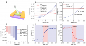
By combining low-energy ion implantation technique with lithography technique, the authors realized patterned doping of 2D materials. The WS2 lateral p-n homojunction was successfully fabricated. “Kelvin probe force microscopy characterizes that there is an obvious surface potential difference in the junction region, and demonstrates the feasibility of constructing lateral p-n homojunction with patterned doping by this method. The p-n junction exhibits significant photovoltaic effect under illumination, and shows satisfactory self-powered photodetection ability under different wavelength lasers. Under 532 nm laser illumination at 1.7 mW cm-2, the self-powered photodetector based on this p-n junction can achieve an open-circuit voltage of 0.39 V, responsivity and detectivity of approximately 35 mA W-1 and 9.8×10¹⁰ Jones.”
They think that “This doping method compatible with integrated circuits shows a huge application potential on modulating the performance of 2D semiconductor devices, and provides a reliable strategy for promoting the practical application of 2D materials.”
DOI
10.1038/s41377-024-01477-3
Original Source URL
https://doi.org/10.1038/s41377-024-01477-3
Funding information
This work was financially supported by the National Natural Science Foundation of China (12025503, U23B2072, 12074293, 12275198), the Fundamental Research Funds for the Center Universities (2042023kf0196).
Lucy Wang
BioDesign Research
email us here
Distribution channels: Science, Technology
Legal Disclaimer:
EIN Presswire provides this news content "as is" without warranty of any kind. We do not accept any responsibility or liability for the accuracy, content, images, videos, licenses, completeness, legality, or reliability of the information contained in this article. If you have any complaints or copyright issues related to this article, kindly contact the author above.
Submit your press release

