

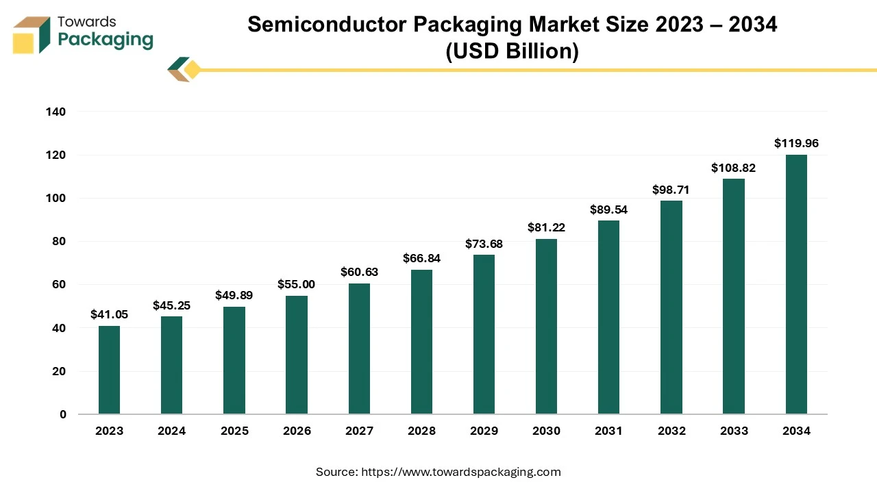
Semiconductor Packaging Market Size to Strike USD 119.96 Bn by 2034
The semiconductor packaging market size stood at US$ 45.25 billion in 2024 and is predicted to exceed US$ 108.82 billion by 2033, experiencing a CAGR of 10.24% from 2024 to 2033.
/EIN News/ -- Ottawa, Feb. 20, 2025 (GLOBE NEWSWIRE) -- The semiconductor packaging market size to record US$ 49.89 billion in 2025 and is projected to grow beyond US$ 119.96 billion by 2034, a study published by Towards Packaging a sister firm of Precedence Statistics.
Access Statistical Data: https://www.towardspackaging.com/download-statistics/5221
Overview of the Market
The semiconductor packaging market is an important segment of the semiconductor industry that focuses on the encapsulation of semiconductor devices. Semiconductor packaging safeguards IC chips from the external environment and ensures their functionality in electronic applications. The market is experiencing significant growth due to the rising demand for high-performance electronic devices.
However, semiconductors are essential for developing high-performance electronic devices, such as wearables, smartphones, and tablets. Semiconductor packaging increases the efficiency of these devices. The growing need for high operating frequency and low power consumption in integrated circuits (ICs) positively impacts the market. Semiconductor packaging can accommodate mechanical stress, heat, and vibration of electronic devices well.
The increasing demand for semiconductors in the IT & telecommunication and automotive industries further contributes to market growth. These industries often require semiconductor devices with high processing power and memory capacity. With the increasing adoption of consumer electronic devices, the demand for semiconductors is rising, further boosting the need for semiconductor packaging to enhance the functionality of these devices. In addition, advancements in semiconductor designing and packing technologies boost the growth of the market.
Join now to access the latest packaging industry segmentation insights with our Annual Membership: https://www.towardspackaging.com/get-an-annual-membership
Major Trends in the Semiconductor Packaging Market:
- Increasing Adoption of AI and 5G Technologies: With the increasing adoption of artificial intelligence (AI) and 5G technologies, the demand for semiconductor packaging that can support increased data rates, working bandwidth, and decreased latency rates increases. Semiconductor manufacturers are exploring new packaging materials and technologies to satisfy such needs. However, system-in-package (SiP) is becoming essential to address the functionality of these technologies.
- High Demand for Eco-friendly Packaging: Manufacturers are increasingly focusing on sourcing sustainable and recyclable materials to manage their product’s effects on the environment. This further minimizes packaging waste and energy consumption.
- Miniaturization of Electronic Devices: There is a growing trend toward smaller and compact electronic devices. As electronic devices become more portable, the need to package multiple chips in a single package increase. However, single packaging also reduces manufacturing costs and energy consumption. Advancements in electronic and communication devices necessitate advanced packaging techniques to cater to the miniaturization of these devices.
- Rising Demand for 3D Packaging: 3D packaging reduces interconnect length, signal delay, and power consumption, making it ideal for high-performance applications like cloud computing and data centers. Moreover, this packaging improves performance and thermal management. With the increasing usage of IoT devices, the demand for advanced packaging solutions, including 3D packaging, that can support connectivity and low power consumption is increasing.
If there's anything you'd like to ask, feel free to get in touch with us @ sales@towardspackaging.com
Insights from Key Regions
Asia’s Sustain Dominance in the Market: What till 2034?
Asia Pacific dominated the semiconductor packaging market with the largest share in 2023. This is mainly due to the increased investments to boost the production of semiconductors. Regional market players have shifted their focus to explore innovative semiconductor packaging materials to fulfill the rising demand for semiconductor packaging. There is a high demand for advanced packaging due to the rising usage of electronic devices, such as smartphones and wearables. Countries like China, South Korea, and Taiwan are known as the manufacturing hubs of electronic devices. As the production of electronic devices increases, manufacturers increasingly demand semiconductor packaging, contributing to regional market growth.
- In May 2023, Taiwan Semiconductor Manufacturing Co., the world’s largest dedicated contract chip maker, revealed that it will build seven facilities to boost its competitiveness globally. These facilities include three wafer plants, two packaging factories located in Taiwan, and two overseas wafer plants.
Rising Adoption of Advanced Technologies to Drives the Market in North America
The semiconductor packaging market in North America is expected to grow at the fastest CAGR during the forecast period. This is mainly due to the increased adoption of advanced technologies. Higher adoption of AI and 5G technologies in the U.S. further contributes to market expansion during the forecast period. North America encompasses some of the world’s largest semiconductor firms, including Intel, Texas Instruments, and Qualcomm.
These companies invest heavily in research and development, accelerating the development of semiconductor packaging. With the rising adoption of high-performance devices, there is a need for advanced packaging solutions, such as 3D packaging, wafer-level packaging, SiP, and heterogeneous integration. However, semiconductor packaging is vital in the effective operation of electronic devices.
- In October 2024, the Biden-Harris Administration issued a Notice of Funding Opportunity (NOFO) funded by the CHIPS and Science Act to enable the United States semiconductor industry to adopt innovative new advanced packaging flows for semiconductor technologies.
Elevate your packaging with Toward Packaging. Improve efficiency and sustainability—schedule a call today: https://www.towardspackaging.com/schedule-meeting
Semiconductor Packaging Market Segmentation
- By material type, the organic substrate segment led the market with the largest share in 2024. This is mainly due to the increased adoption of organic substrates due to their cost-effectiveness and magnificent electrical performance. They are a desirable option for many applications due to their cost benefit.
- By technology type, the traditional segment accounted for the largest market share in 2024. Semiconductor packaging is the method of protecting and connecting semiconductor devices to external circuits. Traditional semiconductor packaging techniques include multilayer ceramic packages, plastic packages, wire bonding technology, and flip chips. Their cost-effectiveness makes them a preferred choice.
-
By end user, the consumer electronics segment dominated the market in 2024. This is mainly due to the increased production of consumer electronic devices like smartphones, tablets, and wearables. However, semiconductor packaging enhances the performance of these devices. The rising miniaturization of electronics further contributes to segmental growth.
Competitive Landscape
The market continues to evolve rapidly, with 2024 witnessing significant advancements and a dynamic competitive landscape. Key players operating in the semiconductor packaging market include HCL Technologies, Moschip Semiconductor Technologies, SPEL Semiconductor, Ruttonsha International Rectifier Ltd, ASE, Amkor Technology, JCET Group, Siliconware Precision Industries Co. Ltd., Powertech Technology Inc., Tianshui Huatian Technology Co. Ltd., Fujitsu Semiconductor Ltd., UTAC, ChipMOS TECHNOLOGIES INC., CHIPBOND Technology Corporation, Intel Corporation, Samsung, Unisem (M) Berhad, Camtek, LG Chem, MIC Electronics Ltd., Surana Telecom and Power Ltd., and Vedanta Ltd. These players are making efforts to hold the maximum share of the market and gain a competitive edge.
- In March 2024, Taiwan Semiconductor Manufacturing Company Limited announced a plan to build an advanced semiconductor packaging factory in Japan. The company is planning to offer its chip-on-wafer-on substrate (CoWoS) packaging technology in Japan. This packaging is useful in increasing operational frequency and decreasing power use in semiconductors.
Recent Developments
- In November 2023, JCET Automotive Electronics (Shanghai) Co., Ltd. received RMB 4.4 billion. The investment is aimed at accelerating the construction of advanced packaging facilities for automotive chip products in the Lingang Special Area of Shanghai.
- In September 2023, Intel Corporation introduced a glass substrate for the next-generation advanced packaging. This glass substrate exhibits properties such as better mechanical and thermal stability and ultra-low flatness, which raises the interconnect density in a substrate. These features of glass substrate help in the production of high-performance, high-density chip packages suitable for data-intensive workloads.
More Insights Towards Packaging:
- The global luxury rigid box market size reached US$ 4.4 billion in 2023 and is projected to hit around US$ 6.70 billion by 2034, expanding at a CAGR of 3.9% during the forecast period from 2024 to 2034.
- The global corrugated bulk bin market size reached US$ 15.3 billion in 2023 and is projected to hit around US$ 26.72 billion by 2034, expanding at a CAGR of 5.2% during the forecast period from 2024 to 2034.
- The global rigid food packaging market size reached US$ 199.50 billion in 2023 and is projected to hit around US$ 341.21 billion by 2034, expanding at a CAGR of 5% during the forecast period from 2024 to 2034.
- The global corrugated wraps market size reached US$ 3.75 billion in 2023 and is projected to hit around US$ 6.28 billion by 2034, expanding at a CAGR of 4.80% during the forecast period from 2024 to 2034.
- The industrial foam market size was USD 62.6 billion in 2023, calculated at USD 66.3 billion in 2024, and is expected to reach around USD 114.6 billion by 2034, expanding at a CAGR of 5.65% from 2024 to 2034.
- The global disposables packaging market size is estimated to reach USD 63.23 billion by 2033, up from USD 36.70 billion in 2023, at a compound annual growth rate (CAGR) of 5.72% from 2024 to 2033.
- The clear plastic tube packaging market size is emerging sector, expected to experience revenue growth and impressive market expansion at a notable CAGR during the forecast period from 2023 to 2034.
- The global collapsible rigid containers market size reached US$ 2.05 billion in 2024 and is projected to hit around US$ 3.69 billion by 2034, expanding at a CAGR of 5.4% during the forecast period from 2024 to 2034.
- The global 3D semiconductor packaging market size reached US$ 11 billion in 2023 and is projected to hit around US$ 57.19 billion by 2034, expanding at a CAGR of 16.17% during the forecast period from 2024 to 2034.
- The cosmetic tubes market size reached US$ 2.99 billion in 2024 and is projected to hit around US$ 4.68 billion by 2034, expanding at a CAGR of 4.61% during the forecast period from 2024 to 2034.
Segments Covered in the Report
By Material Type
- Bonding Wire
- Organic Substrate
- Ceramic Package
- Leadframes
- Encapsulation Resins
- Die Attach Material
- Thermal Interface Materials
- Solder Balls
- Others
By Technology Type
- Advanced Packaging
- Flip Chip
- Embedded Die
- 5D/3D
- SIP
- Fan-in Wafer Level Packaging (FI-WLP)
- Fan-out Wafer Level Packaging (FO-WLP)
- Traditional Packaging
By End Use
- Consumer Electronics
- Automotive
- Healthcare
- IT & Telecommunication
- Aerospace & Defence
- Others
By Region
- North America
- Europe
- Asia Pacific
- Latin America
- Middle East and Africa (MEA)
Review the Full TOC for the Semiconductor Packaging Market Report: https://www.towardspackaging.com/table-of-content/semiconductor-packaging-market-sizing
Invest in Premium Global Insights @ https://www.towardspackaging.com/price/5221
If you have any questions, please feel free to contact us at sales@towardspackaging.com
About Us
Towards Packaging is a leading global consulting firm specializing in providing comprehensive and strategic research solutions. With a highly skilled and experienced consultant team, we offer a wide range of services designed to empower businesses with valuable insights and actionable recommendations. We stay abreast of the latest industry trends and emerging markets to provide our clients with an unrivalled understanding of their respective sectors. We adhere to rigorous research methodologies, combining primary and secondary research to ensure accuracy and reliability. Our data-driven approach and advanced analytics enable us to unearth actionable insights and make informed recommendations. We are committed to delivering excellence in all our endeavours. Our dedication to quality and continuous improvement has earned us the trust and loyalty of clients worldwide.
Browse our Brand-New Journal:
Precedence Research | Statifacts | Towards Healthcare | Towards Automotive | Towards Dental | Towards EV Solutions | Nova One Advisor | Healthcare Webwire | Packaging Webwire | Automotive Webwire
For Latest Update Follow Us: https://www.linkedin.com/company/towards-packaging/

Distribution channels: Business & Economy ...
Legal Disclaimer:
EIN Presswire provides this news content "as is" without warranty of any kind. We do not accept any responsibility or liability for the accuracy, content, images, videos, licenses, completeness, legality, or reliability of the information contained in this article. If you have any complaints or copyright issues related to this article, kindly contact the author above.
Submit your press release