Published on
Apr 15, 2025
Atomic-scale chip alignment: Laser holograms could set new standard for 3D semiconductor overlay accuracy
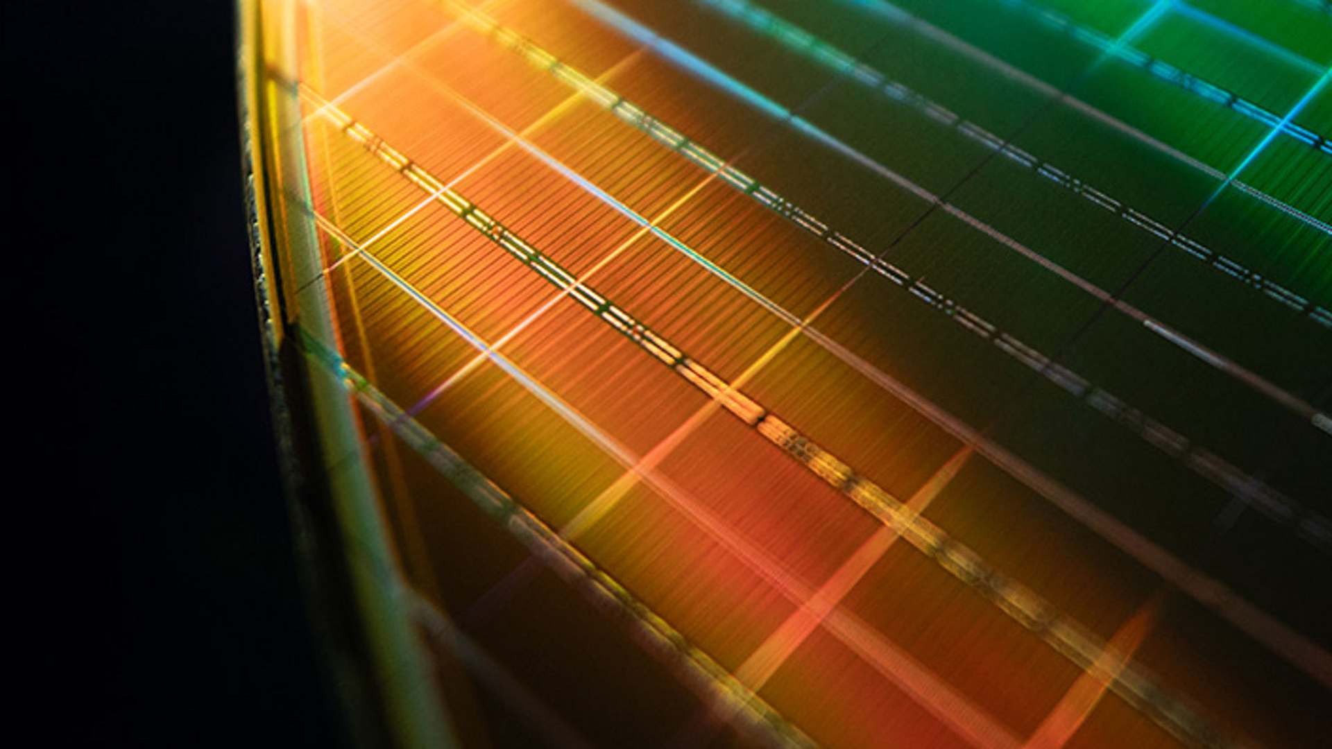
Scientists at the University of Massachusetts Amherst have introduced a novel method for aligning layers in chips using lasers and metalenses. The new technique is claimed to achieve accuracy down to the atomic scale, reports SciTechDaily. This advancement …
Source:
Tom's Hardware
-
Neutral